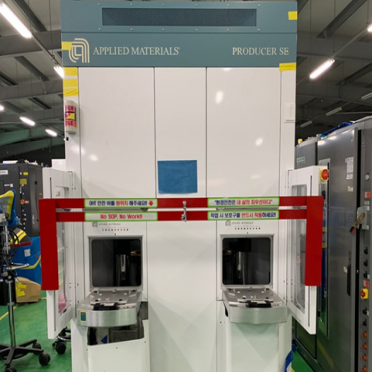
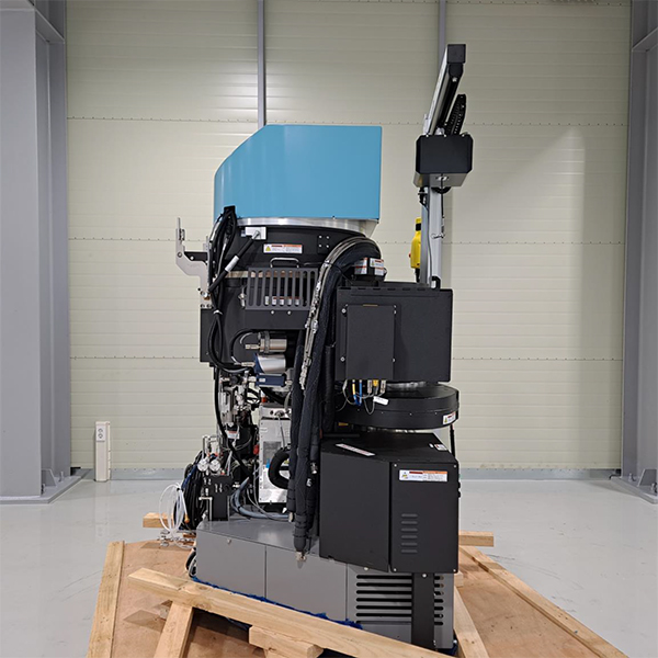
AMAT Centura系列刻蚀设备介绍
Applied Materials Centura Etch system delivers high-productivity silicon, metal, and dielectric etch. Etching is one of the most critical yet challenging of semiconductor production operations. Whether etching a gate, a transistor isolation trench, a high aspect ratio contact, or any level of interconnect metal or dielectric film, maintaining precise, repeatable, and uniform control of critical dimension is the key to device yield. Designed for 150mm and 200mm wafer sizes, the system addresses technology challenges that include high aspect ratio etch ( <110:1) for a range of MtM applications including all-in-one hard mask open-trench-strip for shallow junction MOSFET, and new materials like indium tin oxide, silicon carbide (SiC), InGaAlP, GaAs, and gallium nitride for power devices and LEDs.
The Centura and Centura AP mainframe single-wafer, multi-chamber architectures enable integrated, sequential wafer processing in up to four process chambers for 150mm, 200mm, and 300mm wafers.
For 150/200mm wafers, Applied Centura DPS DTM system employs advanced deep reactive ion etch (DRIE) for a range of materials to precisely control etch wall smoothness and trench profile, while delivering high aspect ratio capability and achieving high throughput. Applied Centura DPS Plus is the industry standard for metal etch processes.
For 200/300mm wafers, Applied Centura AP mainframe chamber technologies address poly, metal, oxide, and DRIE etch.
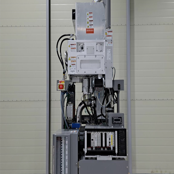
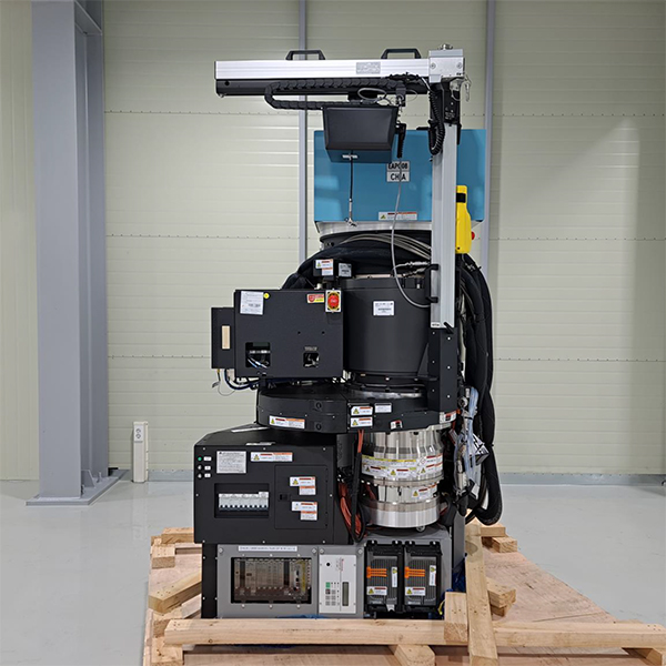
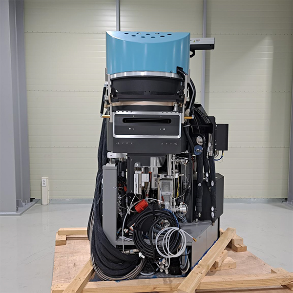
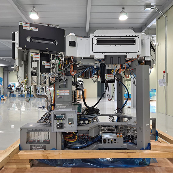
Features:
• Enhanced capabilities for handling a variety of substrates, including III-V materials, reliably and carefully from load lock wafer mapping to clear wafer orientation to wafer placement
• Booster kit with columbic-type ceramic ESC and yttrium-coated process chamber
• EyeD® advanced full-spectrum endpoint and PC Toolset for chamber-state analysis
• Turbomolecular pump for enhanced temperature control of byproducts with blade design to reduce back streaming
• ESC with larger wafer contact area and dual gas feed for better within-wafer performance control
• Top RF source for higher etch rates and in-situ cleans
-
客户为什么选择协宏代加工Services you need we all provide
东莞协宏是一家集亚克力产品开发、模具设计与制造、注塑生产、装配和丝移印为一体的现代化研发型的高新技术企业。公司成立于2000年,拥有现代化亚克力生产设备,在模具设计与制造、注塑成型、成品总装等各项生产制作环节富有先进的技术和成熟的经验,掌握了亚克力制品从设计到生产的全套工艺,享有“全球亚克力制品行业领跑者”荣誉称号。
-

开模-样品试作-量产-成品包装-出荷-全程品质监管
-
客户为什么如此信任协宏的品质matsuga Processing quality
在生产过程中严格依照ISO9001、ISO14001、IATF16949等质量管理体系标准严控产品质量,以品质高、交期快、零退货赢得了客户的信赖与支持。
品质保证部由IQC、PQC、OQC、测量室和信赖性实验室组成。
PQC负责产品各生产环节的品质检查把控;
IQC来料检验及供应商监督;
OQC负责出荷前品质检查,保证每一批产品满足客户的品质要求,零退货;
测量室、信赖性实验室共配备了136台监测设备和实验设备,确保产品在各个生产环节的高品质输出。

客户第一
协宏同仁们始终将客户要求放在第一位,想客户之所想,急客户之所急。第一次把事情做对,已成为每位协宏人做事之准则。
服务优质
协宏公司拥有专职的业务跟单人员、报价工程师,项目工程师,技术工程师。致力于为每位客户提供优质的服务。
团队素养
协宏将“以人为本,以信立业”作为管理理念,我们致力于打造一支团结向上,技术过硬,有活力的团队。以客户为核心,密切关注客户需求。
实力资质
协宏公司20多年行业经验,且有自建的22亩产业园,齐全的自动化设备,完善的质检体系,交期有保障。
- 东莞生产总部
- 武汉生产总部
20多年
行业经验20000㎡
自建厂房36人
研发技术团队150人
生产人员